An audio amplifier or low frequency amplifier, in order to understand how it works and why there are so many transistors, resistors and capacitors, you need to understand how each element works and try to find out how these elements are arranged. In order to assemble a primitive amplifier, we will need three types of electronic elements: resistors, capacitors and, of course, transistors.
Resistor
So, our resistors are characterized by resistance to electric current and this resistance is measured in Ohms. Each electrically conductive metal or metal alloy has its own resistivity. If we take a wire of a certain length with a high resistivity, then we will get a real wirewound resistor. To make the resistor compact, the wire can be wound around the frame. This way we get a wirewound resistor, but it has a number of disadvantages, so resistors are usually made of metal-ceramic material. This is how resistors are designated on electrical diagrams:The upper version of the designation is adopted in the USA, the lower one in Russia and Europe.
Capacitor
A capacitor consists of two metal plates separated by a dielectric. If we apply a constant voltage to these plates, an electric field will appear, which, after turning off the power, will maintain positive and negative charges on the plates, respectively.
The basis of the capacitor design is two conductive plates, between which there is a dielectric
In this way, the capacitor is able to accumulate electrical charge. This ability to accumulate electrical charge is called electrical capacitance, which is the main parameter of a capacitor. Electrical capacitance is measured in Farads. What is also characteristic is that when we charge or discharge a capacitor, an electric current flows through it. But as soon as the capacitor is charged, it stops passing electric current, and this is because the capacitor has accepted the charge of the power source, that is, the potential of the capacitor and the power source are the same, and if there is no potential difference (voltage), there is no electric current. Thus, a charged capacitor does not pass direct electric current, but does allow alternating current, since when connected to an alternating electric current, it will be constantly charged and discharged. On electrical diagrams it is designated as follows:

Transistor
In our amplifier we will use the simplest bipolar transistors. A transistor is made from a semiconductor material. The material property we need is the presence of free carriers of both positive and negative charges. Depending on which charges are greater, semiconductors are divided into two types according to conductivity: n-type and p-type (n-negative, p-positive). Negative charges are electrons released from the outer shells of atoms in the crystal lattice, and positive charges are so-called holes. Holes are vacant spaces remaining in electron shells after electrons leave them. Conventionally, we denote atoms with an electron in the outer orbit by a blue circle with a minus sign, and atoms with a vacant place by an empty circle:
Each bipolar transistor consists of three zones of such semiconductors, these zones are called base, emitter and collector.

Let's look at an example of how a transistor works. To do this, connect two 1.5 and 5 volt batteries to the transistor, with the plus to the emitter and the minus to the base and collector, respectively (see figure):

An electromagnetic field will appear at the contact between the base and emitter, which literally pulls out electrons from the outer orbit of the base atoms and transfers them to the emitter. Free electrons leave behind holes and occupy vacant places already in the emitter. This same electromagnetic field has the same effect on the atoms of the collector, and since the base in the transistor is quite thin relative to the emitter and collector, the collector electrons quite easily pass through it to the emitter, and in much greater quantities than from the base.
If we turn off the voltage from the base, then there will be no electromagnetic field, and the base will act as a dielectric, and the transistor will be closed. Thus, by applying a sufficiently small voltage to the base, we can control the higher voltage applied to the emitter and collector.
The transistor we considered pnp-type, since he has two p-zones and one n-zone. There are also npn-transistors, the principle of operation in them is the same, but the electric current flows in them in the opposite direction than in the transistor we considered. This is how bipolar transistors are indicated on electrical diagrams, the arrow indicates the direction of the current: 
ULF
Well, let's try to design a low-frequency amplifier from all this. First, we need a signal that we will amplify; it can be a computer sound card or any other audio device with a linear output. Let's say our signal with a maximum amplitude of approximately 0.5 volts at a current of 0.2 A, something like this:
And in order for the simplest 4-ohm 10-watt speaker to work, we need to increase the signal amplitude to 6 volts, at current strength I = U / R= 6 / 4 = 1.5 A.
So, let's try to connect our signal to a transistor. Remember our circuit with a transistor and two batteries, now instead of a 1.5 volt battery we have a line output signal. Resistor R1 acts as a load so that there is no short circuit and our transistor does not burn out.

But here two problems arise at once, firstly our transistor npn-type, and opens only when the half-wave value is positive, and closes when the half-wave is negative.

Secondly, a transistor, like any semiconductor device, has nonlinear characteristics in terms of voltage and current, and the lower the current and voltage values, the stronger these distortions:

Not only is there only a half-wave left of our signal, but it will also be distorted:

This is the so-called step-type distortion.
To get rid of these problems, we need to shift our signal to the working area of the transistor, where the entire sinusoid of the signal will fit and nonlinear distortions will be negligible. To do this, a bias voltage, say 1 volt, is applied to the base using a voltage divider made up of two resistors R2 and R3.

And our signal entering the transistor will look like this:

Now we need to remove our useful signal from the collector of the transistor. To do this, install capacitor C1:

As we remember, a capacitor allows alternating current to pass through and does not allow direct current to pass through, so it will serve as a filter that passes only our useful signal - our sine wave. And the constant component that has not passed through the capacitor will be dissipated by resistor R1. Alternating current, our useful signal, will tend to pass through the capacitor, so the resistance of the capacitor for it is negligible compared to resistor R1.
This is the first transistor stage of our amplifier. But there are two more small nuances:
We don’t know 100% what signal is entering the amplifier, what if the signal source is faulty, anything can happen, again static electricity or a constant voltage passes along with the useful signal. This may cause the transistor to not work properly or even cause it to break. To do this, we will install capacitor C2; like capacitor C1, it will block direct electric current, and the limited capacitance of the capacitor will not allow large amplitude peaks to pass through, which can damage the transistor. These power surges usually occur when the device is turned on or off.

And the second nuance is that any signal source requires a certain specific load (resistance). Therefore, the input impedance of the cascade is important for us. To adjust the input resistance, add resistor R4 to the emitter circuit:

Now we know the purpose of each resistor and capacitor in the transistor stage. Let's now try to calculate what element values need to be used for it.
Initial data:
- U= 12 V - supply voltage;
- U bae~ 1 V - Emitter-base voltage of the transistor operating point;

- Pmax= 200 mW - maximum power dissipation;
- Imax= 100 mA - maximum constant collector current;
- Umax= 18 V - maximum permissible voltage collector-base / collector-emitter (We have a supply voltage of 12 V, so there is enough to spare);
- U eb= 5 V - maximum permissible emitter-base voltage (our voltage is 1 volt ± 0.5 volt);
- h21= 75-225 - base current amplification factor, the minimum value is accepted - 75;
- We calculate the maximum static power of the transistor, it is taken 20% less than the maximum power dissipation, so that our transistor does not work at the limit of its capabilities:
P st.max = 0,8*Pmax= 0.8 * 200mW = 160 mW;
- Let's determine the collector current in static mode (without a signal), despite the fact that no voltage is supplied to the base through the transistor, electric current still flows to a small extent.
I k0 =P st.max / U ke, Where U ke- collector-emitter junction voltage. Half of the supply voltage is dissipated on the transistor, the second half will be dissipated on resistors:
U ke = U / 2;
I k0 = P st.max / (U/ 2) = 160 mW / (12V / 2) = 26.7 mA;
- Now let's calculate the load resistance, initially we had one resistor R1, which performed this role, but since we added resistor R4 to increase the input resistance of the cascade, now the load resistance will be the sum of R1 and R4:
R n = R1 + R4, Where R n- total load resistance;
The ratio between R1 and R4 is usually taken to be 1 to 10:
R1 =R4*10;
Let's calculate the load resistance:
R1 + R4 = (U / 2) / I k0= (12V / 2) / 26.7 mA = (12V / 2) / 0.0267 A = 224.7 Ohm;
The closest resistor values are 200 and 27 Ohms. R1= 200 Ohm, a R4= 27 Ohm.
- Now let’s find the voltage at the collector of the transistor without a signal:
U k0 = (U ke0 + I k0 * R4) = (U - I k0 * R1) = (12V -0.0267 A * 200 Ohm) = 6.7 V;
- Transistor control base current:
I b = I to / h21, Where I to- collector current;
I to = (U / R n);
I b = (U / R n) / h21= (12V / (200 Ohm + 27 Ohm)) / 75 = 0.0007 A = 0.07 mA;
- The total base current is determined by the base bias voltage, which is set by the divider R2 And R3. The current specified by the divider should be 5-10 times greater than the base control current ( I b), so that the base control current itself does not affect the bias voltage. Thus, for the current divider value ( I cases) we accept 0.7 mA and calculate R2 And R3:
R2 + R3 = U / I cases= 12V / 0.007 = 1714.3 Ohm
- Now let's calculate the voltage at the emitter at rest of the transistor ( U e):
U e = I k0 * R4= 0.0267 A * 27 Ohm = 0.72 V
Yes, I k0 collector quiescent current, but the same current also passes through the emitter, so I k0 is considered the quiescent current of the entire transistor.
- We calculate the total voltage at the base ( U b) taking into account the bias voltage ( U cm= 1V):
U b = U e + U cm= 0.72 + 1 = 1.72 V
Now, using the voltage divider formula, we find the resistor values R2 And R3:
R3 = (R2 + R3) * U b / U= 1714.3 Ohm * 1.72 V / 12 V = 245.7 Ohm;
The closest resistor value is 250 ohms;
R2 = (R2 + R3) - R3= 1714.3 Ohm - 250 Ohm = 1464.3 Ohm;
We select the resistor value in the direction of decrease, the closest R2= 1.3 kOhm.
- Capacitors C1 And C2 Usually set to at least 5 µF. The capacitance is chosen such that the capacitor does not have time to recharge.
Conclusion
At the output of the cascade, we receive a proportionally amplified signal in both current and voltage, that is, in power. But one stage is not enough for us to achieve the required gain, so we will have to add the next and the next... And so on.The considered calculation is quite superficial and such an amplification circuit, of course, is not used in the construction of amplifiers; we must not forget about the range of transmitted frequencies, distortion and much more.
Ministry of Education of the Russian Federation
Moscow Institute of Physics and Technology
(State University)
Department of Radio Engineering
RF amplifier on bipolar
transistor
Laboratory work
Radio engineering course
Moscow 2003
UDC 621.396.6
Bipolar transistor radio frequency amplifier.
Laboratory work for the course Radio engineering / Comp.
. – M.: MIPT, 2003. – 24 p.
© Moscow Institute of Physics and Technology
State University), 2003
1. Introduction 4
2. Cascade on a bipolar transistor with OE 5
2.1. Circuit diagrams of cascade 5
2.2. Parameters and characteristics of cascade 6
2.3. Selecting cascade parameters in multichannel
amplifier 11
3. Self-excitation of URCH 13
4. Cascode circuit 15
4.1. Circuit diagrams 15
4.2. Circuit parameters and characteristics 16
5. Experimental evaluation of output and input
impedances of the URCH 17 cascade
6. Task 19
6.1. Circuits under study 19
6.2. Calculation of cascades 20
6.3. Measurements and research 21
References 23
1. Introduction
Radio frequency amplifiers (RFA) are widely used in various devices. Most often they are used as input blocks of radio receivers for frequency filtering of the useful signal from interference and increasing its amplitude. In such cases, the central frequency of the signal spectrum, as a rule, significantly exceeds the spectrum width, and then the RF amplifier performs the functions of an active bandpass filter. There are a significant number of similar AMP circuits containing different numbers of amplification elements and frequency-selective circuits. The RF amplifier may contain a single cascade, or it may be multi-stage.
URF is usually described by the following parameters and characteristics:
– resonant (central) frequency of the amplified part of the input voltage spectrum,
– resonant gain https://pandia.ru/text/78/219/images/image003_71.gif" width="23" height="23 src=">
– bandwidth https://pandia.ru/text/78/219/images/image005_58.gif" width="40" height="23">
– input impedance https://pandia.ru/text/78/219/images/image007_51.gif" width="81" height="21">
– output impedance https://pandia.ru/text/78/219/images/image009_42.gif" width="97" height="21">
– amplitude-frequency and phase-frequency characteristics (AFC and PFC).
The purpose of this laboratory work is to theoretically study, calculate, assemble on an individual board and experimentally study the simplest versions of the RF frequency control. This is a resonant cascade on a bipolar transistor connected according to a common emitter (CE) circuit, a cascade circuit on two transistors with one oscillatory circuit, and a two-stage RF frequency converter formed by a series connection of the above cascades.
2. Cascade on a bipolar transistor with OE
2.1. Circuit diagrams of the cascade
In Fig. 1a) shows a schematic electrical diagram of a resonant amplifier cascade based on a bipolar transistor with an OE with a partially switched-on circuit as a collector load and with serial power supply to the collector circuit. In Fig. 1b) shows a diagram of a similar cascade with parallel supply to the collector circuit.
https://pandia.ru/text/78/219/images/image012_34.gif" width="21" height="25"> into the power source, and the alternating component is directed past the source through a capacitor. This reduces unwanted feedback between several cascades of RF power supply, powered from a single source https://pandia.ru/text/78/219/images/image015_28.gif" width="20" height="24">v power source. An inductor (a coil with high inductance), a resistor, or a series connection of an inductor and a resistor are used as impedance.
2.2. Parameters and characteristics of the cascade
The parameters and characteristics of any radio device that describe its properties are usually found by compiling and analyzing the equivalent circuit of this device. For the RF cascade we use an equivalent circuit for alternating current, containing models of the signal source, UE and load. Let's imagine the signal source as a simple voltage generator with EMF and internal resistance ..gif" width="125" height="24 src="> where R– circuit switching factor, – equivalent circuit resistance, ![]() – generalized frequency detuning, https://pandia.ru/text/78/219/images/image024_23.gif" width="17" height="13 src=">1 – intrinsic quality factor of the circuit,
– generalized frequency detuning, https://pandia.ru/text/78/219/images/image024_23.gif" width="17" height="13 src=">1 – intrinsic quality factor of the circuit, ![]() – resonant frequency, – circuit loss resistance connected in series with inductance.
– resonant frequency, – circuit loss resistance connected in series with inductance.
Let us first describe the properties of the cascade with an ideal transistor, whose parameters do not depend on frequency and are equal to: and https://pandia.ru/text/78/219/images/image033_15.gif" width="27" height="28 src =">.jpg" width="397" height="85 src=">
Based on the analysis of this circuit, it is easy to show that the cascade in question has:
– resonant frequency https://pandia.ru/text/78/219/images/image037_13.gif" width="99" height="43"> (1)
where is the transconductance of the transistor,
– resonant gain https://pandia.ru/text/78/219/images/image044_11.gif" width="91" height="23 src=">
– input impedance ![]()
– output impedance to the left of the points https://pandia.ru/text/78/219/images/image048_11.gif" width="73" height="23 src=">
– The frequency response and phase response are specified by the dependence of the modulus and argument of expression (1) on frequency.
At the same time, for a real transistor, the -parameters depend on the frequency. In this work, we will take into account only the so-called first approximation of this dependence, which is valid for frequencies not exceeding several values of the upper limit frequency of the transistor current amplification and has the following form:
https://pandia.ru/text/78/219/images/image053_10.gif" width="156" height="45 src=">
https://pandia.ru/text/78/219/images/image055_10.gif" width="157" height="45 src=">
Here ![]() – forward time constant https://pandia.ru/text/78/219/images/image058_8.gif" width="128" height="23"> – volume resistance of the base, – time constant of the reverse base-collector transition. The approximation corresponds to a physically visual U-shaped equivalent circuit of the transistor (Giacoletto circuit).When used, the equivalent circuit of the cascade takes on the form shown in Fig. 3.
– forward time constant https://pandia.ru/text/78/219/images/image058_8.gif" width="128" height="23"> – volume resistance of the base, – time constant of the reverse base-collector transition. The approximation corresponds to a physically visual U-shaped equivalent circuit of the transistor (Giacoletto circuit).When used, the equivalent circuit of the cascade takes on the form shown in Fig. 3.

In this circuit, in the frequency range of using the RF frequency control, you can ignore the resistor https://pandia.ru/text/78/219/images/image063_9.gif" width="32" height="23 src=">. So, for a transistor KT315 at a frequency of 1 MHz, a capacitance of about three picofarads has an impedance of 50 kOhm, and the value is units of Mohm..gif" width="49" height="23">
Taking into account the above, the results of the analysis of the circuit shown in Fig. 3 boil down to the following.
Output conductance of the part of the cascade located to the left of line K – E, found, for example, as a result of using Norton’s theorem, is equal to
https://pandia.ru/text/78/219/images/image067_8.gif" width="181" height="47 src="> ![]()
![]()
Consequently, the output circuit of the cascade in this case is shunted by the resistor output resistance of the transistor and the output capacitance, the values of which depend on the parameters of the transistor, the output resistance of the signal source and frequency..gif" width="25" height="23 src=">.gif" width ="43" height="21"> we have the order of tens of kOhms and the order of several , and with the order of several kOhms we get the order of (fractions-units) kOhms, and https://pandia.ru/text/78/219/images/image063_9 .gif" width="32" height="23">.
From the equivalent cascade circuit shown in Fig..gif" width="32" height="23">, is equal to where is the impedance of the loaded output circuit https://pandia.ru/text/78/219/images/image080_5.gif " width="136" height="23 src=">.gif" width="29" height="23 src="> Multiplying and dividing the expression for by a complex expression we get ![]() Where ,
Where ,
It follows that the input impedance of the cascade between points B–E is set by the circuit shown in Fig. 4a), where https://pandia.ru/text/78/219/images/image090_6.gif" width="19" height="21 src="> is a parallel connection of resistances and https://pandia.ru/ text/78/219/images/image094.jpg" width="265" height="97">Fig. 4
For transistors with very low resistances, the elements are practically the input resistive resistance of the entire cascade. In the case of large values or in the presence of an additional resistor https://pandia.ru/text/78/219/images/image100_5.gif" width="45 height=15" height="15"> cascade parameters can be found by appropriate recalculation circuit shown in Fig. 4a) into the circuit shown in Fig. 4b), according to the formulas
https://pandia.ru/text/78/219/images/image102_5.gif" width="184" height="43 src=">
Where ![]()
(Note in passing that for frequencies< относительная расстройка имеет знак минус и величина сопротивления https://pandia.ru/text/78/219/images/image010_42.gif" width="24 height=17" height="17">- circuit of any previous stage, the input impedance of the subsequent stage, the resonant frequency and gain of the shunted stage fall, and the bandwidth expands. At the same time, a properly designed cascade should provide the specified values of the entire amplifier and the maximum gain of each stage https://pandia.ru/text/78/219/images/image108.jpg" width="396" height="166">
To ensure the required bandwidth of the cascade, the quality factor of its loaded circuit must be equal to https://pandia.ru/text/78/219/images/image111_4.gif" width="61" height="23 src=">.gif" width ="20" height="23 src="> must satisfy the condition
https://pandia.ru/text/78/219/images/image114_3.gif" width="20" height="21"> and coefficients of connection to the circuit from the output side of the UE cascade and from the input side of the 2nd stage, respectively .
The resonant gain of the cascade from its input to the input of the 2nd stage is equal to
![]() . (3)
. (3)
From expressions (2) and (3) under the condition, the required (optimal) values of the connection coefficients are found
https://pandia.ru/text/78/219/images/image119_4.gif" width="101" height="28 src="> (4)
Where ![]()
A cascade with these connection coefficients is sometimes called optimally matched. The value of the maximum resonant gain of the matched cascade turns out to be equal to
https://pandia.ru/text/78/219/images/image124_4.gif" width="133" height="43 src=">.gif" width="176" height="43 src=">. gif" width="103" height="24"> - the total capacitance of the circuit, providing the resonant frequency of the cascade, equal to the inductance of the circuit coil. From these relations we obtain the following formulas for determining the values of capacitances and https://pandia.ru/text/78 /219/images/image133_3.gif" width="119" height="24">
3. Self-excitation of the URF
Self-excitation of the URF occurs when there is positive feedback in it. There are three channels of such communication. One of them is the connection of cascades through a common power source. To reduce this connection, the cascades are “decoupled” using filter elements and https://pandia.ru/text/78/219/images/image138_3.gif" width="41" height ="23 src=">
Let us consider the conditions under which self-excitation of the RF frequency response occurs precisely because of the named capacitance. They were first discovered by the Russian scientist Vladimir Ivanovich Siforov back in the era of tube radio technology. showed that a single cascade of a resonant amplifier can be excited only if there is an inductive component in its input impedance. Such a component appears, for example, in the presence of a second oscillatory circuit at the input of the cascade. A similar situation arises in a multi-stage amplifier, in which the role of the input circuit of each stage, starting from the second, is played by the output circuit of the previous stage.
In Fig. Figure 6 shows a simplified equivalent circuit of a cascade with two identical circuits, which are represented in it by two-terminal networks with impedances ![]() these circuits (taking into account their shunting by a transistor). The UE is represented by a current generator. Capacitance is the throughput capacity of the cascade.
these circuits (taking into account their shunting by a transistor). The UE is represented by a current generator. Capacitance is the throughput capacity of the cascade.

Let's break the circuit wire at a point and apply a harmonic input voltage https://pandia.ru/text/78/219/images/image144_3.gif" width="15" height="15 src="> to the cascade, which will cause an output voltage ![]() Under the influence of the sum of the input and output voltages, a feedback current will flow through the pass capacitance. At large cascade gains, the contribution of the input voltage can be neglected and we can assume that https://pandia.ru/text/78/219/images/image148_2.gif" width= "29" height="21 src="> If the initial phases of the voltages turn out to be equal, and the amplitude of the coupling voltage exceeds the amplitude https://pandia.ru/text/78/219/images/image150_2.gif" width="111" height="23">when we also have At this frequency the impedances of both circuits are inductive. If at the resonant frequency the voltages and are in antiphase (the shift is equal to https://pandia.ru/text/78/219/images/image154_2.gif" width="17" height="21"> the phase shift between the voltages and is already equal to the phase shift between the vectors and is equal to and the shift between the vectors and is equal to As a result, the phase shift between the voltages and turns out to be equal to zero, that is, the feedback becomes purely positive.If the second (amplitude) condition is also satisfied, then the RF amplifier cascade turns into an inductive three- dot https://pandia.ru/text/78/219/images/image160_2.gif" width="21" height="24">
Under the influence of the sum of the input and output voltages, a feedback current will flow through the pass capacitance. At large cascade gains, the contribution of the input voltage can be neglected and we can assume that https://pandia.ru/text/78/219/images/image148_2.gif" width= "29" height="21 src="> If the initial phases of the voltages turn out to be equal, and the amplitude of the coupling voltage exceeds the amplitude https://pandia.ru/text/78/219/images/image150_2.gif" width="111" height="23">when we also have At this frequency the impedances of both circuits are inductive. If at the resonant frequency the voltages and are in antiphase (the shift is equal to https://pandia.ru/text/78/219/images/image154_2.gif" width="17" height="21"> the phase shift between the voltages and is already equal to the phase shift between the vectors and is equal to and the shift between the vectors and is equal to As a result, the phase shift between the voltages and turns out to be equal to zero, that is, the feedback becomes purely positive.If the second (amplitude) condition is also satisfied, then the RF amplifier cascade turns into an inductive three- dot https://pandia.ru/text/78/219/images/image160_2.gif" width="21" height="24">
For the stability of the URF, it is necessary that the voltage amplitude be less than the voltage amplitude https://pandia.ru/text/78/219/images/image162_2.gif" width="85 height=25" height="25"> (7)
Thus, expression (7) indicates ways to combat self-excitation due to the presence of a pass-through capacitance of the UE. These are the corresponding restrictions on quantities and
4. Cascode circuit
4.1. Circuit diagrams
The cascode circuit is designed to increase the resistance of the amplifier to self-excitation, which is achieved by significantly reducing its throughput capacity compared to the minimum achievable throughput capacity of a separate UE. Examples of cascode circuits with serial and parallel DC power supply are given in Fig. 7.

4.2. Circuit parameters and characteristics
As can be seen from these figures, the load of the 1st transistor, connected according to a circuit with a OE, in alternating current is the input impedance of the 2nd transistor, connected according to a circuit with a common base (CB). Since the value of such impedance is very small compared to the output impedance of the 1st transistor (the 1st transistor of the cascode circuit practically operates in short circuit mode at its output, and the 2nd transistor operates in idle mode at its input. In addition, we have
If we now consider both transistors of the cascode circuit as a single UE, then under the specified conditions its -parameters are related to the similar parameters of the 1st and 2nd transistors by the following relations
https://pandia.ru/text/78/219/images/image171_2.gif" width="32" height="23 src=">.gif" width="55" height="23 src=">
https://pandia.ru/text/78/219/images/image175_2.gif" width="96" height="23 src=">.gif" width="21" height="23"> cascode circuit, estimating the degree of feedback through the pass capacitance turns out to be much less than that of a single transistor connected in a circuit with an OE. This makes the cascode circuit more resistant to self-excitation.
In addition, due to the small value, the input impedance of the cascode circuit is equal to the 1st transistor,
and the output impedance is equal to https://pandia.ru/text/78/219/images/image180_2.gif" width="37" height="21">.gif" width="19 height=21" height="21 "> unloaded circuit. Theoretical calculation of these quantities is cumbersome and inaccurate, so we will describe the method for their experimental assessment.
Values https://pandia.ru/text/78/219/images/image075_6.gif" width="33" height="21 src=">.gif" width="27" height="23 src="> determined by the total capacity of the circuit + WITH P, where WITH P is the known capacity of a suspended capacitor pre-installed in the circuit. We calculate the value using the formula
https://pandia.ru/text/78/219/images/image182_2.gif" width="72" height="43 src="> (8)
Where ![]() .
.
Changing the capacity WITH We tune the cascade to the required resonant frequency and measure its bandwidth. After this, we partially connect the capacitive branch of the circuit to the collector of the transistor, as shown in the equivalent circuit of this connection in Fig. 8a). In this case, we select the values of the capacitors so that, taking into account the known capacitance, the resonant frequency of the cascade is equal to https://pandia.ru/text/78/219/images/image186_2.gif" width="15" height="16">= ( 0.2–0.8).In the linear mode of operation of the cascade, we measure its bandwidth, the resonant frequency of the 1st stage without connecting the 2nd stage to it was equal to Calculate the value
d) assuming that for all transistors h 21E = 100, find their initial base currents I bn = I book/ h 21E,
e) select the current flowing through a voltage divider made up of resistors R 1 and R 2, equal I d = (50–100) I bn, find values R 1 and R 2, also taking into account the condition that the transistor base potential VT3 relative to the ground should be equal to ( U ken + 0.6 V),
e) find the quantities R R, R b1, R f, R b2.
6.2.2. AC calculation:
a) take two coils with equal inductances (40–60) μH from the cash register, measure their inductances at https://pandia.ru/text/78/219/images/image024_23.gif" width="17" height="13 src="> L;
b) set the preliminary value of the coefficient of partial connection of the 1st circuit p= (0.25–0.33), determined by the ratio of its capacities;
c) calculate the capacitance values of both circuits;
d) select the capacitance of the remaining capacitors of the circuit on the order of (0.01–1) μF, thereby ensuring the required smallness of their impedance at the resonant frequency.
6.3. Measurements and research
6.3.1. Study of single cascades
On the student’s individual board, assemble a cascade on a transistor with an OE, connecting its circuit completely to the transistor, connecting points 3 and 4 using a decoupling capacitor WITH R. Assemble a cascode circuit, leaving its input (point 6) free. Measure real values I book and U ken of both cascades and check their compliance with the specified values. If necessary, achieve compliance with an accuracy of (10–25)% by changing the values R b1, R b2, R 1 and R 2.
By connecting a radio frequency harmonic voltage generator with an amplitude of no more than 20 mV to the input of the 1st stage (points 1 and 2), and a voltmeter to points 5 and 2, measure the resonant frequency of this stage and check its compliance with the calculated value https://pandia.ru /text/78/219/images/image018_26.gif" width="20" height="21 src="> on the frequency response and phase response of the cascade on a transistor with OE.
6.3.2. Study of two-stage RF frequency control
Using the measurement results in paragraph 6.3.1, materials
2.3 and formulas (4)–(6), calculate the parameters of a matched cascade on a transistor with an OE loaded by a cascode circuit. In this case, set the required bandwidth of the 1st stage equal to its bandwidth when the circuit is fully turned on and in the absence of connection to the 2nd stage.
Assemble the described two-stage amplifier. If there is self-excitation, take measures to eliminate generation.
For a stable two-stage amplifier in its linear mode of operation, measure the values of the resonant gain and passbands of the 1st stage and the entire amplifier as a whole.
When preparing for the test at home and preparing the report:
a) master the derivation of calculation formulas (4), (8), (9)–(11),
b) compare the obtained values of all measured quantities with the theoretically expected ones.
Bibliography
1.
Basics of radio electronics. – M.: Radio and Communications, 1990.
2. ,
Radio receiving devices. In 2 hours - M.: Sov. radio, 1961–1963.
Laboratory work
Current consumption - 46 mA. The bias voltage V bjas determines the output power level (gain) of the amplifier

Fig. 33.11. Internal structure and pinout of TSH690, TSH691 microcircuits

Rice. 33.12. Typical inclusion of TSH690, TSH691 microcircuits as an amplifier in the frequency band 300-7000 MHz
and can be adjusted within 0-5.5 (6.0) V. The transmission coefficient of the TSH690 (TSH691) microcircuit at a bias voltage V bias = 2.7 V and a load resistance of 50 Ohms in a frequency band up to 450 MHz is 23 (43) dB, up to 900(950) MHz - 17(23) dB.
Practical inclusion of TSH690, TSH691 microcircuits is shown in Fig. 33.12. Recommended element values: C1=C5=100-1000 pF; C2=C4=1000 pF; C3=0.01 µF; L1 150 nH; L2 56 nH for frequencies not exceeding 450 MHz and 10 nH for frequencies up to 900 MHz. Resistor R1 can be used to regulate the output power level (can be used for an automatic output power control system).
The broadband INA50311 (Fig. 33.13), manufactured by Hewlett Packard, is intended for use in mobile communications equipment, as well as in consumer electronic equipment, for example, as an antenna amplifier or radio frequency amplifier. The operating range of the amplifier is 50-2500 MHz. Supply voltage - 5 V with current consumption up to 17 mA. Average gain

Rice. 33.13. internal structure of the ΙΝΑ50311 microcircuit
10 dB. The maximum signal power supplied to the input at a frequency of 900 MHz is no more than 10 mW. Noise figure 3.4 dB.
A typical connection of the ΙΝΑ50311 microcircuit when powered by a 78LO05 voltage stabilizer is shown in Fig. 33.14.

Rice. 33.14. broadband amplifier on the INA50311 chip
Shustov M. A., Circuitry. 500 devices on analog chips. - St. Petersburg: Science and Technology, 2013. -352 p.
Aperiodic RF frequencies only increase the signal-to-noise ratio and receiver sensitivity. They are most often used in direct amplification transistor receivers in the LW and SW ranges; As a load of aperiodic RF units, it can
Fig.9. Circuits of aperiodic stages of radio frequency amplifiers:
a) – resistor; b) – transformer.
serve as a choke, resistor or transformer. Resistor cascade of RF amplifier (Fig. 9. a ) is easy to implement and configure. In transformer URCHs (Fig. 9.b ) it is easier to match the output of one stage with the input of the next one. In addition, the transformer cascade of the RF amplifier can be easily converted into a reflex cascade.
Resonant amplifiers provide signal amplification and increase not only real sensitivity, but also selectivity in the mirror channel. Transistor resonant amplifiers in the DV, MV and KB ranges are assembled according to a circuit with OE (Fig. 10 ), and in the VHF range - according to the scheme with OB.
Cascades of RF amplifiers can contain one or two resonant circuits. A single-loop RF amplifier produces less gain but is easier to manufacture and configure. Inductively coupled circuits allow you to vary the coupling and obtain the highest gain or best selectivity. By changing the connection over the range, you can somewhat compensate for the unevenness of the transmission coefficient of the input circuits.
VHF radio frequency amplifiers are made using cascade circuits. They have better characteristics than conventional URCHs.
In terms of gain, a cascode amplifier is equivalent to a single cascade amplifier with the direct transmission conductivity of the first transistor and the load of the second. The cascode circuit is used in meter wave amplifiers. It is advantageous to implement the first stage of the circuit on a field-effect transistor, which has a low noise level and low active input conductivity, and the selective system of the receiver, connected at the input of the cascode amplifier, will be less shunted. In the second stage, a drift transistor is preferred, connected according to the circuit with ABOUT and providing the highest stable gain.
Fig. 10. RF amplifier stage.
With this design of the amplifier's cascode circuit, its stable gain increases, the noise level is significantly reduced, and the selectivity of the receiver's radio signal path increases, which is their advantage. Similar advantages are offered by cascode circuits (low noise level and high stable gain) using electron tubes, usually triodes, connected according to the common cathode - common grid circuit.
The principle of superheterodyne reception.
Detection and amplification of low frequency signals.
To increase the sensitivity and real selectivity of a heterodyne receiver, the input circuit must provide a power transfer coefficient close to unity in the operating frequency range and the greatest possible attenuation of out-of-band signals. All these are properties of an ideal bandpass filter, therefore the input circuit must be designed in the form of a filter.
The often used single-circuit input circuit is the least suitable for meeting the requirements. To increase selectivity, it is necessary to increase the loaded quality factor of the circuit, weakening its connection with the antenna and mixer or amplifier.
But then almost all the power of the received signal will be spent in the circuit and only a small part of it will pass into the mixer or amplifier. The power transfer coefficient will be low. If you strongly connect the circuit to the antenna and mixer, the loaded quality factor of the circuit will drop and it will little attenuate the signals of stations neighboring in frequency.
But very powerful radio broadcasting stations operate next to the amateur bands.
A single input circuit as a preselector can be used on low-frequency HF bands, where signal levels are quite high, in the simplest heterodyne receivers. The connection with the antenna should be made adjustable, and the circuit itself tunable, as shown in Fig. 1.
In case of interference from powerful stations, you can weaken the connection with the antenna by reducing the capacitance of capacitor C1, thereby increasing the selectivity of the circuit and at the same time increasing the losses in it, which is equivalent to turning on the attenuator. The total capacitance of capacitors C2 and SZ is chosen to be about 300...700 pF, these coils depend on the range.
Fig.1. Single-circuit input circuit.
Significantly better results are obtained by bandpass filters matched across the input and output. In recent years, there has been a tendency to use switchable bandpass filters even at the input of wide-range professional communications receivers. Octave (rarely), half-octave and quarter-octave filters are used.
The ratio of the upper frequency of their passband to the lower one is respectively 2; 1.41 (root of 2) and 1.19 (fourth root of 2). Of course, the narrower the input filters, the higher the noise immunity of the wide-range receiver, but the number of switchable filters increases significantly.
For receivers designed only for amateur bands, the number of input filters is equal to the number of bands, and their bandwidth is selected equal to the band width, usually with a margin of 10...30%.
In transceivers, it is advisable to install bandpass filters between the antenna and the antenna transmit/receive switch. If the transceiver's power amplifier is quite wide-bandwidth, as is the case with a transistor amplifier, its output signal may contain many harmonics and other out-of-band signals. A bandpass filter will help suppress them.
The requirement for a filter power transfer coefficient close to unity is especially important in this case. The filter elements must withstand reactive power several times greater than the rated power of the transceiver transmitter.
It is advisable to choose the characteristic impedance of all band filters to be the same and equal to the characteristic impedance of the feeder of 50 or 75 Ohms.

Fig.2. Bandpass filters: a - L-shaped; b - U-shaped
The classic circuit of an L-shaped bandpass filter is shown in Fig. 2, a. Its calculation is extremely simple. First, the equivalent quality factor Q = fo/2Df is determined, where fo is the average frequency of the range, 2Df is the filter bandwidth. The inductance and capacitance of the filter are found according to the formulas:
where R is the characteristic resistance of the filter.
At the input and output, the filter must be loaded with resistances equal to the characteristic resistance, these can be the input resistance of the receiver (or output transmitter) and the antenna resistance.
A mismatch of up to 10...20% has practically little effect on the characteristics of the filter, but the difference between the load resistance and the characteristic resistance by several times sharply distorts the selectivity curve, mainly in the passband.
If the load resistance is less than the characteristic value, it can be connected via an autotransformer to the tap of the L2 coil. The resistance will decrease by a factor of k2, where k is the switching factor equal to the ratio of the number of turns from the tap to the common wire to the total number of turns of the L2 coil.
The selectivity of one L-shaped link may not be sufficient, then two links are connected in series. The links can be connected either by parallel branches to each other, or by sequential ones. In the first case, a T-shaped filter is obtained, in the second - a U-shaped one.
The L and C elements of the connected branches are combined. As an example, Fig. 2b shows a U-shaped bandpass filter. Elements L2C2 remained the same, and elements of the longitudinal branches were combined into inductance 2L and capacitance C1/2. It is easy to see that the tuning frequency of the resulting series circuit (as well as the rest of the filter circuits) remained the same and equal to the average frequency of the range.
Often, when calculating narrow-band filters, the value of the capacitance of the longitudinal branch C1/2 turns out to be too small, and the inductance too large. In this case, the longitudinal branch can be connected to the taps of the L2 coils, increasing the capacitance by 1/k2 times, and reducing the inductance by the same amount.
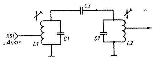
Fig.3. Double-circuit filter.
In high-voltage filters, it is convenient to use only parallel oscillatory circuits connected by one terminal to a common wire.
The circuit of a two-circuit filter with external capacitive coupling is shown in Fig. 3. The inductance and capacitance of parallel circuits are calculated using formulas (1) for L2 and C2, and the capacitance of the coupling capacitor should be C3=C2/Q.
The switching coefficients of the filter outputs depend on the required input resistance Rin and the characteristic resistance of the filter R: k2=Rin/R. The switching coefficients on both sides of the filter can be different, ensuring coordination with the antenna and the receiver input or transmitter output.
To increase selectivity, three or more identical circuits can be connected according to the diagram in Fig. 3, reducing the capacitance of the SZ coupling capacitors by 1.4 times.
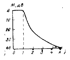
Fig.4. Selectivity of a three-circuit filter.
The theoretical selectivity curve of a three-circuit filter is shown in Fig. 4. The relative detuning x=2DfQ/fo is plotted horizontally, and the attenuation introduced by the filter is vertically plotted.
In the transparency band (x<1) ослабление равно нулю, а коэффициент передачи мощности - единице. Это понятно, если учесть, что теоретическая кривая построена для элементов без потерь, имеющих бесконечную конструктивную добротность.
A real filter also introduces some attenuation in the passband, which is associated with losses in the filter elements, mainly in the coils. Losses in the filter decrease as the design quality factor of the Q0 coils increases. For example, with Q0 = 20Q, losses even in a three-circuit filter do not exceed 1 dB.
Attenuation outside the passband is directly related to the number of filter circuits. For a double-circuit filter, the attenuation is equal to 2/3 of that indicated in Fig. 4, and for a single-circuit input circuit - 1/3. For the U-shaped filter Fig. 3, b, the selectivity curve Fig. 4 is suitable without any correction.
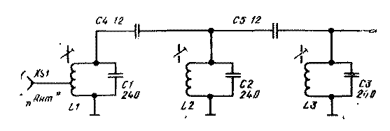
Fig.5. Three-circuit filter - practical circuit.
The practical circuit of a three-circuit filter with a passband of 7.0...7.5 MHz and its experimentally measured characteristics are shown in Fig. 5 and 6, respectively.
The filter was calculated according to the described method for a resistance of R = 1.3 kOhm, but was loaded onto the input resistance of the heterodyne receiver mixer of 2 kOhm. Selectivity increased slightly, but peaks and dips appeared in the passband.
The filter coils are wound turn to turn on frames with a diameter of 10 mm using PEL 0.8 wire and contain 10 turns. The tap of coil L1 to match the antenna feeder resistance of 75 Ohms is made from the second turn.
All three coils are enclosed in separate screens (aluminum cylindrical “cups” from nine-pin lamp panels). Setting up the filter is simple and comes down to adjusting the circuits to resonance using coil trimmers.
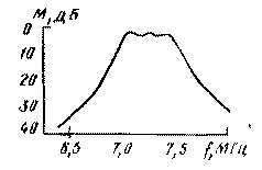
Fig.6. Measured selectivity curve of a three-circuit filter.
Particular attention should be paid to the issues of obtaining the maximum design quality factor of filter coils. One should not strive for special miniaturization, since the quality factor increases with increasing geometric dimensions of the coil.
For the same reason, it is not advisable to use too thin a wire. Silvering the wire gives a noticeable effect only at high frequencies. KB bands and on VHF when the design quality factor of the coil is more than 100. Litz wire is advisable to use only for winding coils in the ranges of 160 and 80 m.
Lower losses in silver-plated wire and Litz wire are due to the fact that high-frequency currents do not penetrate into the thickness of the metal, but flow only in a thin surface layer of the wire (the so-called skin effect).
An ideally conducting screen does not reduce the quality factor of the coil and also eliminates energy loss in objects surrounding the coil. Real screens introduce some losses, so it is advisable to choose the screen diameter equal to at least 2-3 coil diameters.
The screen should be made of highly conductive material(copper, somewhat worse than aluminum). Painting or tinning the internal surfaces of the screen is not permitted.
The listed measures ensure exceptionally high quality factor of the coils, which is realized, for example, in spiral resonators.
In the 144 MHz range it can reach 700...1000. Figure 7 shows the design of a two-resonator 144 MHz bandpass filter designed for inclusion in a 75-ohm feedline.
The resonators are mounted in rectangular screens with dimensions of 25X25X50 mm, soldered from sheet copper, brass or double-sided foil fiberglass plates.
The internal partition has a connection hole measuring 6X12.5 mm. Air tuning capacitors are mounted on one of the end walls, the rotors of which are connected to the screen.
The resonator coils are frameless. They are made of silver-plated wire with a diameter of 1.5...2 mm and have 6 turns with a diameter of 15 mm, evenly stretched to a length of about 35 mm. One terminal of the coil is soldered to the stator of the trimmer capacitor, the other to the screen.
The taps to the filter inlet and outlet are made from 0.5 turns of each coil. The bandwidth of the tuned filter is slightly more than 2 MHz, the insertion loss is calculated in tenths of a decibel. The filter bandwidth can be adjusted by changing the size of the coupling hole and selecting the position of the coil taps.
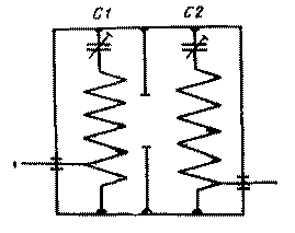
Fig.7. Filter on spiral resonators.
At higher frequency VHF bands, it is advisable to replace the coil with a straight piece of wire or tube, then the spiral resonator turns into a coaxial quarter-wave resonator loaded with capacitance.
The length of the resonator can be selected around l/8, and the length missing up to a quarter of the wavelength is compensated by a tuning capacitance.
In especially difficult reception conditions on the HF bands, the input circuit or filter of the heterodyne receiver is made narrow-band and tunable. To obtain a high loaded quality factor and a narrow band, the connection with the antenna and between the circuits is chosen to be minimal, and to compensate for the increased losses, an AMP on a field-effect transistor is used.
Its gate circuit does little shunting of the circuit and almost does not reduce its quality factor. It is not advisable to install bipolar transistors in the URF due to their low input resistance and significantly greater nonlinearity.
URCH scheme
The radio frequency amplifier (RFA) circuit is shown in Fig. 8. A two-circuit tunable bandpass filter at its input provides all the required selectivity, therefore, a non-tunable low-Q circuit L3C9, shunted by resistor R3, is included in the drain circuit of the transistor.
This resistor is used to select the cascade gain. Due to the low gain, neutralization of the transistor pass capacitance is not required.
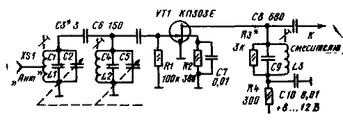
Fig.8. Radio frequency amplifier.
The circuit in the drain circuit can also be used to obtain additional selectivity if the shunt resistor is eliminated, and to reduce the gain, the drain of the transistor is connected to the tap of the loop coil.
The diagram of such an AMP for the 10 m range is shown in Fig. 9. It provides a receiver sensitivity of better than 0.25 µV. The amplifier can use dual-gate transistors KP306, KP350 and KP326, which have a low pass-through capacitance, which contributes to the stability of the operation of the RF amplifier with a resonant load.

Fig.9. URCH on a two-gate transistor.
The transistor mode is set by selecting resistors R1 and R3 so that the current consumed from the power source is 4... 7 mA. The gain is adjusted by moving the tap of coil L3 and when the coil is fully turned on it reaches 20 dB.
Contour coils L2 and L3 are wound on K10X6X4 rings made of 30HF ferrite and have 16 turns of PELSHO 0.25 wire. The communication coils with the antenna and mixer each contain 3-5 turns of the same wire. It is easy to introduce an AGC signal into the amplifier by applying it to the second gate of the transistor. When the potential of the second gate is reduced to zero, the gain decreases by 40...50 dB.
Literature: V.T. Polyakov. Radio amateurs about direct conversion technology. M. 1990